Coding Up a Device PCB Design
TL;DR This post describes my project to knock some of the risk out of circuit board design. I try out a new way of writing code to design circuit boards. I develop an approach to shift between debug and production versions of circuit boards without introducing new errors, and use it to make a new device.
How It Started
My name is Dylan Jackson. I’m an electrical engineer who, through no fault of my own, ended up specializing in embedded system design. I’ve worked on infrared imaging systems, robots that manage(d) solar farms, energy monitoring systems, and designed this COPD-monitoring medical device (currently in production):

Since shifting to more contracting, I’ve worked on a host of other budding startup products that are on their way to the market in one way or another. In the last couple of years alone I’ve had maybe 4-5 different projects instead of just one. This means I’m doing a lot more new electrical designs, rather than iterating (obsessing?) over one or two.
How It’s Going
Well I love developing hardware so, good! Mostly. While the prospect of building new designs is really exciting, the reality is clunky. Even if I had bothered to create lovely nice project templates to get Altium (my preferred PCB CAD software) set up, I find that I’m building a lot of the same circuits from scratch every time. An LDO and a couple of capacitors isn’t so bad to redo, but battery chargers and fuel gauges have a lot more supporting circuitry. Even if I’ve used the part before, I still have to consult the datasheet for every little detail (where’s that resistor table that sets the current limit again?). In the best case that’s just kind of annoying, but sometimes it can really mess things up.
See, the fun thing about hardware is that when I make a mistake, I find out after a week or two of sitting on my hands and hundreds/thousands of dollars in parts and manufacturing costs. It’s even more fun if the mistake is related to a part I’ve used successfully before 🙃.
This is not to say embedded software doesn’t have its own challenges (IT DOES), but at least that C function I wrote to convert twos-complement to decimal floats will still work if I try to use it on another project. More importantly, I can just copy it easily without much risk. Reduced risk means fewer mistakes, which leads to shorter timelines, less cost, and happier clients.
If I copy a circuit from another Altium project, the net names might not line up with the rest of the schematic. That might not sound like a big deal, but it has bitten me before. ”CDC1_INT” and “INT_CDC1” can both seem like good conventions at different times (to say nothing of “VDD” vs “VCC”). Here I’m trying to reuse schematic sheets for a sensor and a BLE SoC, and the alternating net-naming conventions I used at different times are not doing me any favors.
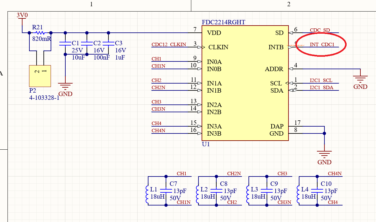
Note the INT_CDC# convention here
.png)
Note the different CDC#_INT convention here. Those nets would not be connected!
I want to find a way to re-use circuits the way I could re-use a C function. I do not want to waste time re-reading the same datasheets and exposing myself to risk every time I start a new design with elements I’ve already used successfully in the past.
My goal is to figure out a hardware design flow that:
- Makes it easy to actually reuse my design work. Just copying and pasting schematic sheets is too error prone.
- Reduces the cost and risk of errors in circuit board development. I have a lot of projects that would benefit from a custom circuit board, but often the appetite from my customer isn’t there. The risk of adding circuit board development to a project is perceived as very high, and I want to lower it.
- Lets me switch between debug and release versions of hardware designs. I use proof of concept, and evaluation boards to test new ideas and new components in order to derisk a circuit board design. I want to smash those debug boards into a production version without incorporating any new errors.
HaaS (Hardware as a Software)
I decided to try JITX, which provides a way to design circuit board schematics with a programming language instead of “by hand” in my CAD program.
Being a bit more hardware focused I’m always afraid of anything that isn’t vanilla C, but it was late enough in the pandemic that I had already run out of active dry yeast and I suddenly had all this extra time on my hands! So I decided to give it a go with a new design I had coming up.
The first step was to see how easily I could define components in code. In Altium, everything is graphically defined, but in JITX, my design is code. The library is code, the symbols are code, and the footprints are code. Here’s a snippet that defines a resistor, and its visualization in JITX:
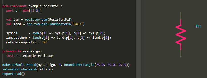
This code defines a new resistor component, sets up a design with that resistor, and exports it to Altium. resistor-sym and ipc-two-pin-landpattern are parametric functions that create the resistor symbol and an 0402 landpattern.
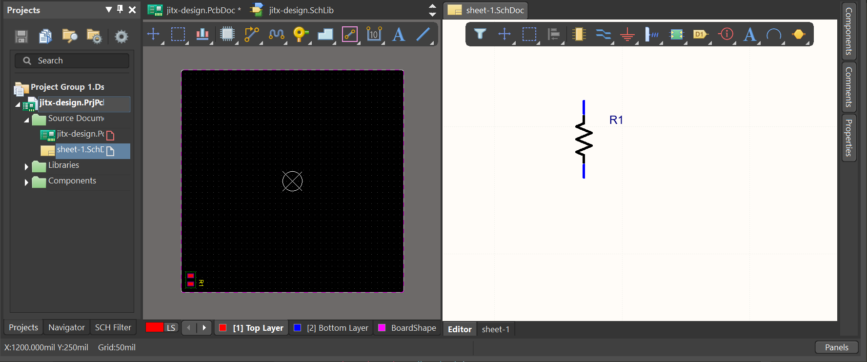
When I run this code in JITX it creates this Altium project:
At first it felt weird writing code to describe something I always intuited as being physical, but with any new language/technology/software you have to stick with it a little bit to get to the power it provides. And like any new tool, I found JITX had something of a learning curve to it. Figuring out the syntax and how to properly use the code-based drawing functions to make footprints took a bit of getting used to, but it turns out there are quite a few neat tricks you can do when describing a component in code.
What really stuck out to me was the ability to define modules. As a simple example, a linear voltage regulator might have a recommended input and output capacitor of 1uF. If I define a module that includes those capacitors along with the regulator, I don’t have to look back at that datasheet every time to check. I just make the module once and then I’m good to use it later.

This module is an LDO with its input and output stabilizing caps. bypass-cap-strap is a convenience function that pulls a capacitor with specified parameters (just speccing 1.0 uF here) from a database, attaches it between two pins, and adds an annotation for layout.
These modules (including the base components) can also be parametric, which is really cool. If a (buck) converter has a variable output voltage set by a resistor value, the module can be written to include a different resistor value depending on what the output voltage argument is when the module is instantiated. Because it’s all code you can really parametrize any aspect of the part/module, including footprints, passive component values, etc.
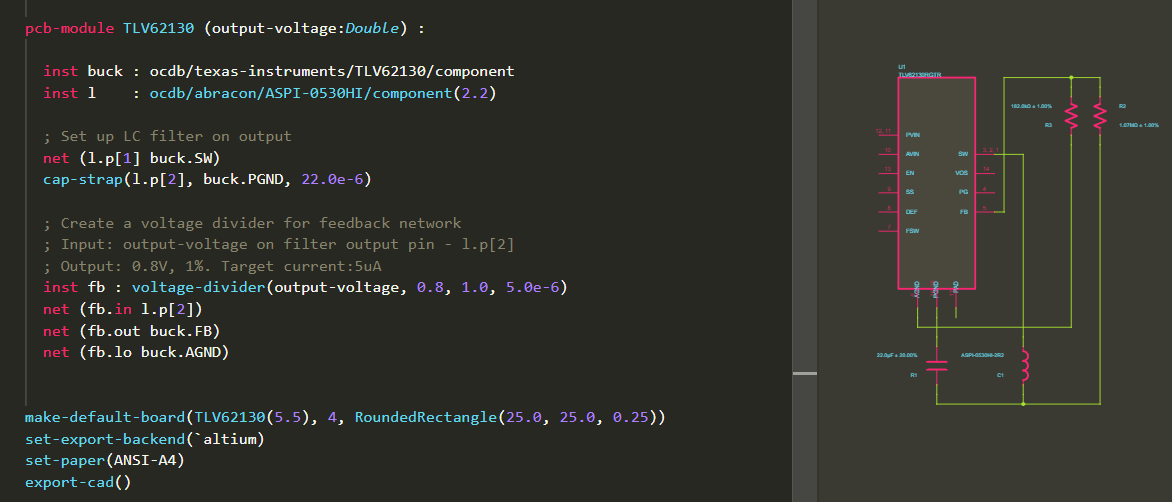
This module sets up a buck regulator to be parametric in the output voltage. The regulator adjusts the output voltage to maintain 0.8V on the FB pin, we use a voltage divider to provide that feedback. make-voltage-divider is a function that finds a pair of in-stock standard value resistors for the divider that meet design requirements for accuracy and total current.
It also has a feature called “bundles”, which allowed me to group a series of connections together and treat it like a single entity. I use this feature to connect multiple devices to a single I2C bus, or a SPI bus between two devices (without having to worry about net names!)
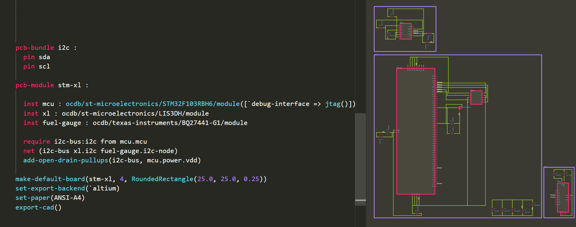
I can use the i2c bundle to connect the sda and scl pins across a microcontroller, an accelerometer, and a battery fuel gauge. require just finds a set of pins on the microcontroller that support i2c, and the add-open-drain-pullups function adds a pair of pullup resistors based on the speed and capacitance of the i2c bus.
Which exports to Altium as:
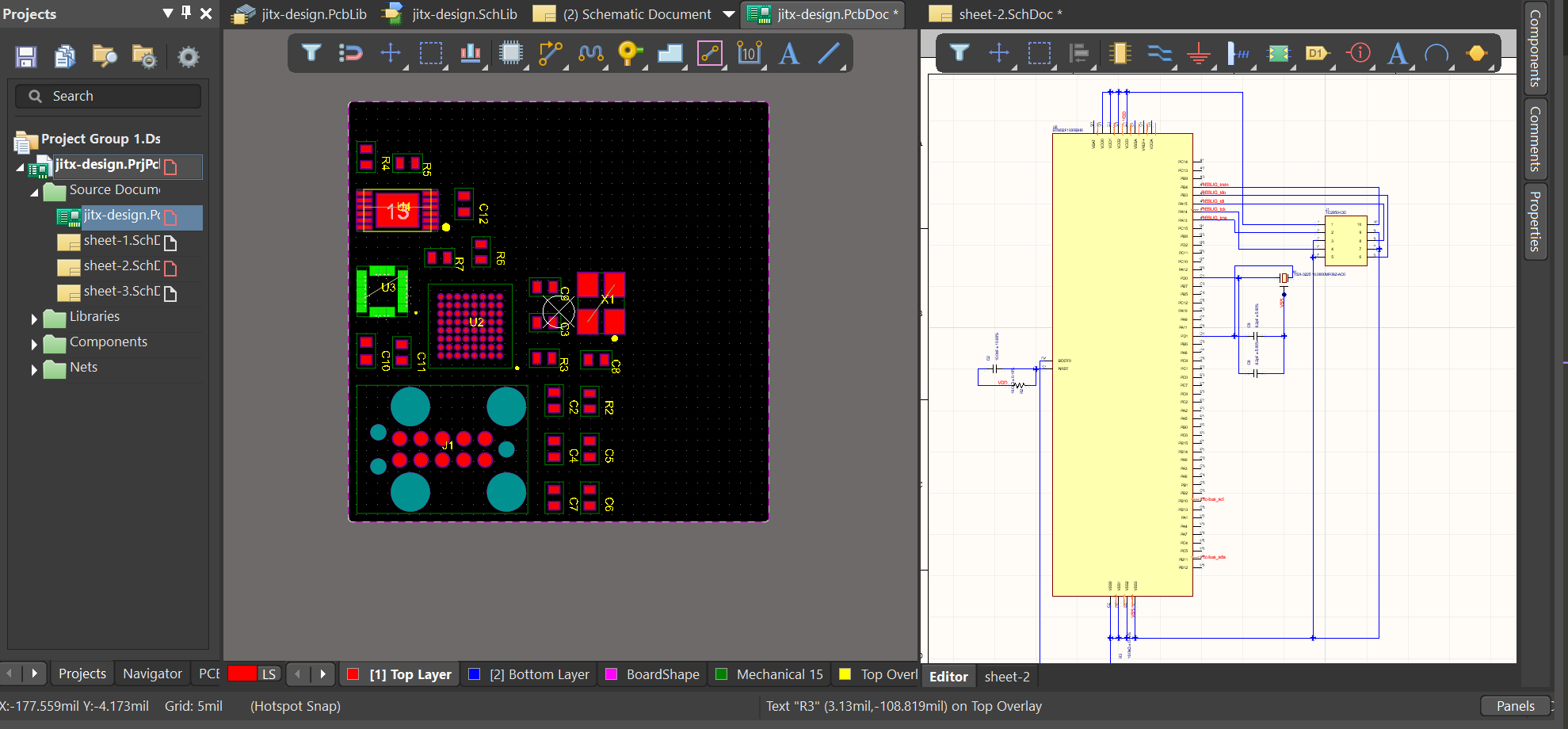
To clarify the process flow a little bit, JITX is acting as the tool for generating the schematic, defining which pins on what parts are connected to what other pins on other parts. The output file from JITX gets imported to another CAD program (Altium Designer, in my case) for layout (the “physical” placing of parts and drawing the copper traces that make those connections).
I have to say, going from the traditional method where each connection is made by hand to giving general connection instructions via code is exciting, but not without some trepidation. It removes a lot of time and point-and-click tedium compared to the usual method, but it also requires that I trust that the mcu module was built correctly and that the code really does connect my i2c bus to compatible pins (or at least that I will get a compilation error if it does not). After all, the whole point is to make it so that I can spend less time checking the datasheets manually and simultaneously reduce the likelihood of a mistake. Even with traditional CAD software I still double/triple check everything anyway, so I suppose it’s not much different in that respect.
It’s worth mentioning that JITX does allow me to be as prescriptive as I want about connections. I can specify individual pins instead of letting JITX assign them, but it’s certainly a fairly powerful capability. I think the only reason I might assign pins manually is to simplify routing on a microcontroller (e.g. putting the I2C pins on the side facing most of the rest of the chips on the bus), but that’s also an optimization I typically don’t get to until I start routing anyway.
Moving From Debug To Release Hardware
With this software-based approach up my sleeve, I wanted to see if it could meet my goals for my new design flow. I had an imminent project involving a client who was building a new IoT product to monitor blood pressure. Most of the system was composed of known quantities (e.g. BLE SoC, battery charger, accelerometer, etc), but the client had a really cool novel sensor, so I wasn’t sure which interfacing IC would work best.
There were a few candidate chips I wanted to be able to evaluate, so I thought I would build two PCBs: a motherboard with the known-stuff and a daughterboard with whatever IC I wanted to try. They would be connected by a header large enough to contain power, ground, I2C, SPI, and a few GPIO for good measure. After I settled on an IC, I would make a smaller board that consolidated the two proto-designs into one “final” design.
I was starting with something like this:
Trying to end up with something like this:
I prefer this style of approach for most projects (whether it’s motherboard + daughterboard, or big, broken-out development board) because making mistakes in hardware is expensive. It means another costly board run plus your own time figuring out what the problems are (and the time goes way up if you went for your compact final design first). So this should be a risk reduction measure, but converting between these designs is very much its own process. That conversion process has risk of its own. In other words, while development boards remove some risk, they merely move the rest of the risk to the eventual “releasification” of the design.
For instance, net names need to be consistent and nets separated by a 2-pin header/jumper (which I use all the time in development builds to measure current) need to be reconnected. On a big schematic, it can be easy to miss one, which is all it takes to cause problems. Just ask my, uh, “friend”, who once missed a net connection going from a debug design to a form-factor design and had to do some time-consuming and unsightly rework to fix it
Contrast that to when I write firmware, switching between debug and release versions is much safer and more streamlined. I’ll often have some code wrapped in debug #define statements that only gets compiled when I want to run the “debug version”. When I want to run the normal version, all that stuff gets left out.
Now that I’m using this software-based hardware design, maybe that could help me set things up in a similar way? Then I could build a development version for evaluating components and then easily generate the production version without the possibility for errors. Without risking botching the merging of the two.
Remember that “bundles” feature? Well it’s not at all constrained to a set of common connections (e.g. I2C, SPI). I defined a bundle (”b2b”) that was the set of connections between the two boards, which should allow me to simply connect the bundles together and all of the connections within will be handled automatically, like so.
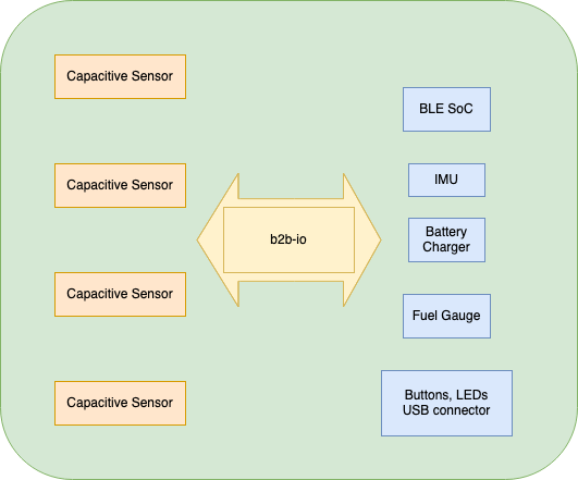
Previously those connections were to physical headers on the separate boards, so setting up those connections just looked something like this:
pcb-bundle b2b-io :
  port spi-b2b : spi-controller()
  port i2c-b2b : i2c
  pin vcc
  pin gnd

  port gpioCtrl : pin[[ 1 through 9]]
  port gpioInt : pin[[ 1 through 3]]

pcb-module nrf-mother :
  port b2b : b2b-io
  ...
  net spi (b2b.spi-b2b, nrf52.spi-master, imu.spi-node)
  net i2c (b2b.i2c-b2b, nrf52.i2c-master)
  net gpioINT1 (b2b.gpioInt1, nrf52.P1[08])
  net gpioINT2 (b2b.gpioInt2, nrf52.P0[07])
  net gpioINT3 (b2b.gpioInt3, nrf52.P0[17])
Note that the b2b bundle was written to contain i2c and spi bundles, in addition to basic GPIO connections, just like you could make a struct in C that contains other structs as well as standard types.
I designed (and manufactured) the separate mother and daughter board PCBs using JITX. Each design was its own module, which I exported to Altium, and routed by hand:
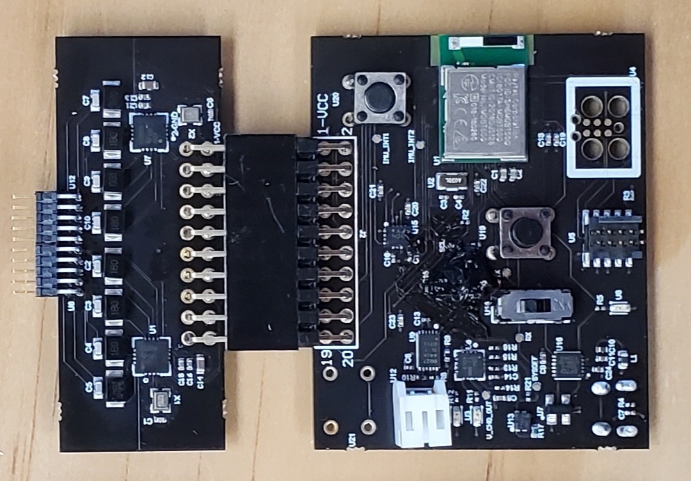
Motherboard (right) and daughterboard (left) joined by the aforementioned b2b header
Because each previous PCB was its own “module”, the merged design was literally just this:
pcb-module nrf52-fd2214-merged:
  inst nrf : nrf-mother
  inst sense : cdc-daughter

  net (nrf.b2b, sense.b2b)
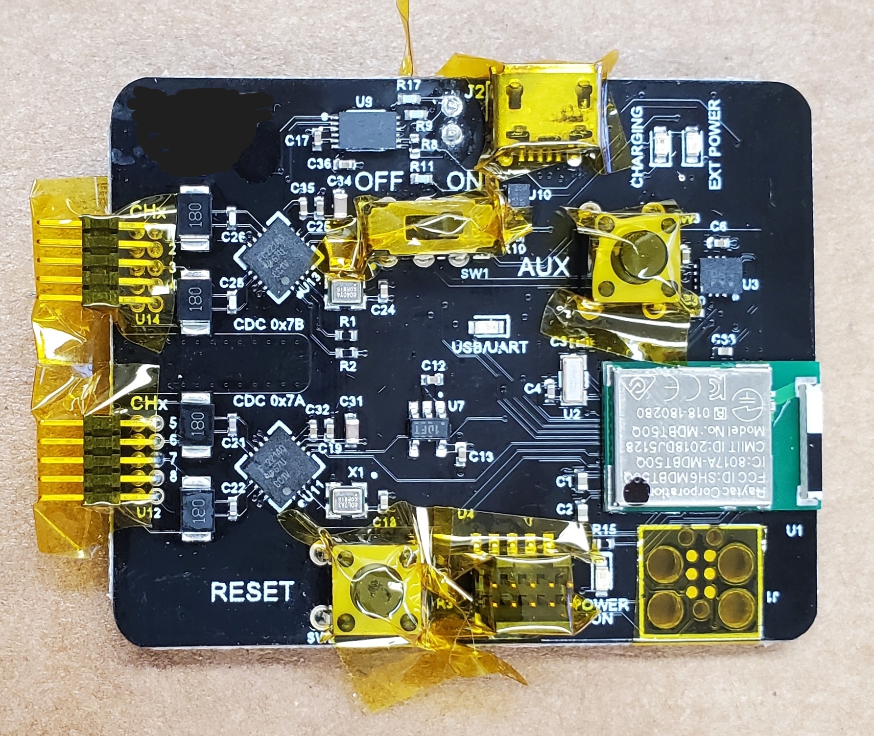
Merged design (with Kapton tape masking for the conformal coating I was about to spray).
I thought that was really cool. It’s conceptually exactly the same as putting two small, single-IC modules on one PCB, but you can make a “module” anything you want, including an entire design.
So the flow worked! I was able to get my debug to release process going for circuit board designs, and my client was happy enough to opt for more hardware projects in the future.
How It Ended
In the end, I was able to create a couple of designs, including that mother-daughter board pair, export them to Altium and everything came out fine (except for a “small” pinout mistake, but I didn’t need JITX’s help for that). Merging the designs into a smaller form-factor board was a piece of cake with the bundles feature. In the process, I built reusable circuit modules that I could easily use with later designs.
There are a lot of other really cool things that a software-driven hardware approach enables that I haven’t covered here (like using loops to create multiple elements/connections/pads). It’s a compelling technology that I think really shines when iterating on a design or re-using common elements in multiple designs. It is also a new technology and very much being actively developed and improved. I believe it now supports importing component libraries (which is HUGE in terms of lowering friction of use) and I expect it will only keep getting better. Admittedly, I haven’t fully integrated this new design flow yet (partly because I’ve been doing more “not PCB design” lately) but I think there’s something really worthwhile there and I definitely want to keep exploring it.


